What is a Photonic Integrated Circuit?
Editor’s note: This article was originally published on the PhotonDelta website in December 2022. It is reposted here with their permission.
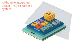
A photonic integrated circuit (PIC) is a microchip containing two or more photonic components which form a functioning circuit, hence also called photonic chip.
Photonic components utilize photons (or particles of light) as opposed to electrons. As they move at the speed of light, photons have a wide bandwidth and minimal energy loss, making them both fast at transferring data and highly energy efficient.
Photonic integrated circuits can be used to create faster, and more energy efficient devices. That’s because these PICs can sense with the highest level of precision, and are highly effective at processing and transmitting data. They are also integrated alongside traditional electronic chips and applications across a range of industries, including data and telecommunications, medical and healthcare, engineering and transport.
The history of integrated photonics
Photonics is the science behind the detection, generation, and manipulation of light particles (photons). According to quantum mechanics and the concept of wave-particle duality first proposed by Albert Einstein in 1905, light acts as both an electromagnetic wave and a particle. The context in which light is operating determines the nature of light observed. For example, light bending through a lens takes a wave form whereas in fibre optics, light takes particle form as a photon, which carries no mass and a specific amount of energy.
Integrated photonics (IP) is a branch of photonics in which multiple photonic functions and waveguides are fabricated on the surface of a flat substrate made from either Indium Phosphide (InP), Silicon Nitride (SiN), or Silicon Photonics (SiPh). This breakthrough in technology means that photonic integrated circuits can now process and transmit light similarly to how electronic integrated circuits conduct electrical signals.
A few highlights
Integrated circuits using electrical components were first developed in the late 1940s and early 1950s, but it took until 1958 for them to become commercially available. When the laser and laser diode were invented in the 1960s, the term ‘photonics’ fell into more common usage to describe the application of light to replace applications previously achieved through the use of electronics.
By the 1980s, photonics gained traction through its role in fibre optic communication. At the start of the decade, an assistant in a new research group at Delft University Of Technology, Meint Smit, started pioneering in the field of integrated photonics. He is credited with inventing the Arrayed Waveguide Grating (AWG): a core component of modern digital connections for the Internet and phones.
Ton Backx was the founder and first director of the Institute for Photonic Integration and CEO of PhotonDelta. Under his leadership, the Electrical Engineering department grew to be the largest in the Netherlands in the years before. Backx has been appointed Knight in the Order of the Netherlands Lion.
How does a photonic integrated circuit work?
A photonic integrated circuit works by using photons (particles of light) to transfer, sense, process, and transmit information. Using waveguides to control and direct light through total internal reflection, photonic integrated circuits are comparable to the wires used to carry electrical signals. A laser source provides the light needed to drive the components, similar to a switch in an electrical circuit.
Connected by waveguides, multiple components can be integrated and fabricated on a single substrate to create robust and miniaturised solutions. Components in the photonic integrated circuit can be both passive and active. Examples of passive components are switches and multiplexers. Active components include detectors and lasers.
The differences between photonics and electronics
Photonics is similar to electronics. However, instead of electrons, it uses photons to transfer information. Whilst electronics refers to the control of electrons on a microchip, photonics refers to the control of photons. A photonic integrated circuit is comparable to an electronic integrated circuit (IC) but there are some significant differences between the two:
- A photonic integrated circuit provides functions for information signals imposed on optical wavelengths, typically in the visible spectrum or near infrared 850 nm-1650 nm.
- Electrical components require a switch to turn to connect an electrical supply and active electrical components, whereas photonic components are activated by a light source (a laser).
- Integrated circuits conduct electricity by enabling a flow of negatively-charged electrons through a circuit. A photonic integrated circuit allows the flow of photons.
- Electrons interact with other particles which causes them to move slowly through copper wires, generates heat, and causes energy loss. Travelling at the speed of light, photons are virtually frictionless and therefore faster and more energy efficient.
- In terms of fabrication, in an electrical circuit the transistor is the dominating component, whereas in photonic integrated circuits there is no dominating device.
What problems do photonic integrated circuits solve?
As global data consumption rises and demand for faster networks continues to grow, the world needs to find more sustainable solutions to the energy crisis and climate change. At the same time, ever more innovative applications for sensor technology, such as Lidar in autonomous driving vehicles, appear on the market. There is a need to keep pace with technological challenges.
The expansion of 5G data networks and data centres, safer autonomous driving vehicles, and more efficient food production cannot be sustainably met by electronic microchip technology alone. However, combining electrical devices with integrated photonics by heterogeneous integration provides a more energy efficient way to increase the speed and capacity of data networks, reduce costs and meet an increasingly diverse range of needs across various industries.
Which industries and applications use PICs?
One of the first examples of photonic integrated circuits is a 2-section Distributed Bragg Reflector (DBR) laser, consisting of two independently controlled device sections: a gain section and a DBR mirror section.
Today, there are growing numbers of industries and applications for photonic integrated chips as designers tackle evermore challenging technological problems by incorporating photonic technology into their solutions.

Telecommunications
The primary application for PICs is in the area of fibre-optic communication. The arrayed waveguide grating (AWG), which are commonly used as optical (de)multiplexers in wavelength division multiplexed (DWDM) fibre-optic communication systems, are an example of a photonic integrated circuit. Another example in fibre-optic communication systems is the externally modulated laser (EML) which combines a distributed feedback laser diode with an electro-absorption modulator. For instance, EFFECT Photonics addresses the need for high-performance and affordable optical communications solutions, such as SPF+ optical transceivers, which help meet the demand for bandwidth and faster data transfer.
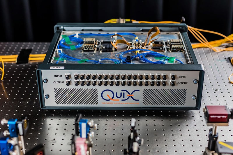
Not only can PICs increase bandwidth and data transfer speeds, they can reduce energy consumption in data centres, which spend a large proportion of energy on cooling servers. Compared with solely electronic solutions, PICs generate far less heat and can mitigate the need for cooling, reducing energy consumption. For example, QuiX Quantum develops quantum photonic processors which enable photonic quantum computers to operate at room temperature – a major step forward in reducing their cost and size.
Healthcare
Using photonic biosensors and creating more affordable diagnostic biomedical instruments, integrated photonics opens the door to the very real possibility of lab-on-a-chip (LOC) technology, cutting waiting times, and taking diagnosis out of laboratories and into the hands of doctors and patients. Based on an ultrasensitive photonic biosensor, SurfiX Diagnostics’ plug-and-play diagnostics platform provides a variety of point-of-care tests. Similarly, Amazec Photonics has developed a fibre optic sensing technology with photonic chips which enables high-resolution temperature sensing (fractions of 0.1 milliKelvin) without having to inject the temperature sensor within the body. This way, medical specialists are able to measure both cardiac output and circulating blood volume from outside the body. Another example of optical sensor technology is EFI’s OptiGrip device, which offers greater control over tissue feeling for minimal invasive surgery.
Transport & Engineering
In automotive integrated photonics can be used to monitor the surroundings of vehicles through sensor systems like Lidar (light detection and ranging). It can also be deployed in-car connectivity through Li-Fi, which is similar to WiFi but uses light. This technology also facilitates communication between vehicles and urban infrastructure to improve driver safety. For example, some modern vehicles pick up traffic signs and remind the driver of the speed limit. In terms of engineering, fibre optic sensors can be used to detect different quantities, such as pressure, temperature, vibrations, accelerations, and mechanical strain. Sensing technology from PhotonFirst uses integrated photonics to measure things like shape changes in aeroplanes, electric vehicle battery temperature, and infrastructure strain.
Food production
Sensors play a vital role in revolutionizing agriculture and the wider food industry in order to reduce wastage and detect diseases. Light sensing technology powered by PICs can measure variables beyond the range of the human eye, allowing the food supply chain to detect disease, ripeness and nutrients in fruit and plants. It can also help food producers to determine soil quality and plant growth, as well as measuring CO2 emissions. A new, miniaturised, near-infrared sensor, developed by MantiSpectra, is small enough to fit into a smartphone, and can analyse the chemical content of milk and plastics.
Types of fabrication and materials
The most commercially utilised material platform for photonic integrated circuits is Indium Phosphide (InP), which allows for the integration of various optically active and passive functions on the same chip. The fabrication techniques are similar to those used in electronic integrated circuits and uses photolithography pattern wafers for etching and material deposition.
The platforms considered most versatile are Indium Phosphide (InP), Silicon Nitride (SiN) and Silicon Photonics (SiPh):
- Indium Phosphide (InP) PICs have active laser generation, amplification, control, and detection. This makes them an ideal component for communication and sensing applications.
- Silicon Nitride (SiN) PICs have a vast spectral range and ultra low-loss waveguide. This makes them highly suited to detectors, spectrometers, biosensors, and quantum computers. The lowest propagation losses reported in SiN (0.1 dB/cm down to 0.1 dB/m) have been achieved by LioniX International’s TriPleX® waveguides.
- Silicon Photonics (SiPh) PICs provide low losses for passive components like waveguides and can be used in minuscule photonic circuits. They are compatible with existing electronic fabrication.
Silicon Photonics actually refers to the technology rather than the material. It combines high density photonic integrated circuits (PICs) with complementary metal-oxide-semiconductor (CMOS) electronics fabrication. The most technologically mature and commercially used platform is Silicon on Insulator (SOI).
Other platforms include:
- Lithium Niobate (LiNbO3) is an ideal modulator for low loss mode. It’s highly effective at matching fibre input-output due to its low index and broad transparency window. For more complex PICs, Lithium Niobate can be formed into large crystals. As part of project ELENA, there is a European initiative to stimulate production of LiNbO3-PICs. Attempts are also being made to develop ‘Lithium Niobate on Insulator (LNOI).
- Silica has a low weight and small form factor. It’s a common component of optical communication networks, such as Planar Light wave Circuits (PLCs).
- Gallium Arsenide (GaAS) has high electron mobility. This means GaAS transistors operate at high speeds, making them ideal analogue integrated circuit drivers for high speed lasers and modulators.
By combining and configuring different chip types (including existing electronic chips) in a hybrid or heterogeneous integration, it is possible to leverage the strengths of each. Taking this complementary approach to integration addresses the demand for increasingly sophisticated energy-efficient solutions.
Where are photonic integrated circuits developed and produced?
The most notable academic centres of excellence for photonic integrated circuits are the University of California, Santa Barbara in the US, and the Eindhoven University Of Technology and the University of Twente in the Netherlands.
Public-private partnerships, such as PhotonDelta and the American Institute for Manufacturing Integrated Photonics (AIM Photonics), also provide end-to-end supply chains and ecosystems to help kickstart and scale companies working within integrated photonics.
There are a number of organiszations specializing in different types of fabrication:
- Smart Photonics is a foundry for Indium Phosphide (InP)
- LioniX International is an organization specializing in Silicon Nitride (SiN)
- Ligentec is a foundry for Silicon Nitride (SiN)
- AMF and VTT are foundries for Silicon Photonics (SiPh)
- GlobalFoundaries, and TowerSemiconductors are foundries for semiconductors Silicon Photonics (SiPh)
- Imec has a pilot line for Silicon Photonics (SiPh)
About HighTechXL
HighTechXL is the Netherlands’ premier deep-tech venture builder, solving societal challenges by combining groundbreaking technologies and entrepreneurship. We bring together and activate technology, talent, funding and a strong ecosystem in our unique Venture Building Program.
News